Having complained about the Peavey PC1600's small memory, I decided to do something about it. Having done something about it I'm here to share the knowledge.
This hack makes it seem like you have two Peavey PC1600s in the same box - twice the scenes, twice the presets etc. etc. A PC3200 in fact.
The hack is not elegant, in fact, depending on which method you use to implement it, it is downright crude; but it works. However before I tell you how to do it I want to make a few things clear.
I will of course benefit from the warm thoughts you have about me when you successfully carry out this hack and come to realise how way cool it is, and what a mondo homeboy I am (or somesuch).
OK that's the scary disclaimer stuff dealt with, here is what to do. First of all you need to obtain two memory chips. My Peavey PC1600 had a Sony component CXK58257AP-70LL in it. This is now obsolete and unsupported by Sony, although you may still be able to obtain it from their distributors.
Toshiba make an equivalent chip TC55257DPL-70L and you should be able to get this fairly readily, for something like 4 bucks a piece (they cost £2.34 in the UK).
I got two memory chips and did the hack with these leaving the original memory chip unchanged, in case I wanted to revert the hack, I suggest you do the same, and this description assumes this is what you have done.
You will also need a "subminiature" double-pole, double-throw (DPDT) switch. This is also known as a double-pole changeover (DPCO) switch. You can use a lever, or a slider type. The slider type looks a little more discrete. Depending which method you adopt you may need some other parts described below.
There are three activities that are required for both methods of this hack. To reduce duplication I put these below, ahead of the methods. The methods contain links back to these sections.
You need to avoid zapping the memory chips, or your PC1600 with static electricity. Wear an antistatic wrist strap (for example "3M 2209 disposable wrist strap"). Ensure the other end is connected to something you know to be earthed/grounded. From now on you should be able to handle the chips without blowing them up.
You will have to open up your Peavey PC1600 and get it ready for the hack, but you will probably not need to do this until after you have followed one of the methods below.
Save your PC1600 presets to some external storage (computer, sysex utility, sequencer, another PC1600 etc.).
Disconnect the power lead to the Peavey PC1600 and any other cables. Open it up by removing the six screws around the edge (three front, three back), and gently separate the base cover from the top.
Turn the top part of the case upside down so that you can see the logic board. Place it so that the MIDI sockets are furthest from you and the display circuit board is on your left.
Gently remove the existing RAM chip. On my board this was marked "U104", and was below a "Varta" 3.6 volt battery. Place the RAM chip in an antistatic carrier for safe keeping.
Next decide where your switch will go. If you use the first method, and the switch is mounted on the PCB, you will be constrained to the position the switch rests in when the PCB is mounted, and you will have to determine this position once the pcb is built and you are ready to install it. Otherwise, if you use the cheapo method, you can probably put the switch wherever it fits and suits you.
Mark out or measure a slot/hole for your switch on the rear panel of the PC1600 and carefully cut this hole out of the panel. Be careful that no swarf (little metal drillings or filings) remains in the machine.
Whichever method you choose, once the hack has been performed you will need to intialise the PC1600.
Turn the Peavey PC1600 right way up, and arrange the switch so that you can operate it. Reconnect the power lead, hold down the "Utility" and "Enter" buttons while you turn the thing on. This initialises it. Check that it still works. Then turn it off. Switch your RAM selecting switch and repeat the initialising procedure (you've got two PC1600s now and you need to initialise both of them).
Re-install the presets you saved earlier.
In addition to the two memory chips and switch, you will need a 28-way ribbon cable about nine inches, or 25 cm long terminated at each end with a 28-way DIL plug header. The 28-pin plug headers are available as 3M part no. 3728 - 4000T. This is available from Mouser in the 'States as stock no. 517-3278-4000. A similar thing can be obtained from Maplin in the UK as stock no. JP40T. The standard cable near this size has 34 strands so you would need to strip off six strands from the unmarked edge before fitting the connectors. You will also need a pcb (details below) and two 28-pin DIL IC sockets.
I have produced a PCB layout. It is an Adobe Acrobat pdf. The layout is scaled 2:1 (ie it's twice as big as the final board), so you will need to print the layout onto an acetate sheet and then get a friendly PC board manufacturer (look in Yellow Pages) to photo-reduce it and make a board up for you. I used a crummy cheapo drawing program to make the layout and the transition to pdf has not improved it. You will probably have to ensure that none of the tracks on the PCB (especially those near the switch) is shorting, by running a fine scalpel between the tracks.
In fact I printed this layout at 1:1 straight from the drawing program, onto one of those laser printable etch resistant overlays and made my own PCB. The product I used was called "Press-n-Peel" (grim name or what?), and I got this from Maplin (stock no. AB15). It's made by a company In the UK but I guess there are similar products elsewhere in the world. Having printed onto the "p-n-p" you then iron it onto a lump of copperclad board, with a standard domestic clothes iron. Then you etch the board with Ferric Chloride solution. Sounds quick and easy but it's not.
I found this p-n-p stuff really critical and it took me about three goes before the transfer worked. If the iron is too hot the layout gets blobbed up and fills in between tracks; if it is too cold, the tracks don't stick to the copper, or worse still, they look like they have but the etchant gets underneath them and eats up what should be a track. Ferric chloride is a nasty substance to have hanging around the house - especially if you have kids around.
So, if you are really desperate to do the whole thing yourself, you could reduce the layout in a photocopier and copy it onto a similar product. But I really wouldn't recommend it. It's just a lot of hassle. Getting the 2:1 layout made up by a professional will cost about £35 or about 50 bucks.
Once you've got your pcb, by fair means or foul, the first job is to solder the header at one end of the ribbon cable into the PCB.
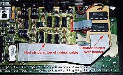
This requires a surprising amount of thought to get right. The cable will probably have a red edge. This edge represents the pin 1 end of the headers. If it does not then you should identify pin 1 on the header for yourself. Place the cable in front of you with the red (or pin 1) edge at the top (ie furthest away from you). The header on the right-hand end of the cable is the one which goes in the PCB. Now place the PCB in front of you track side down, with the switch area on your left-hand side. The ribbon cable header goes into the rightmost set of holes. The cable will then run over the top of the PCB to the left, covering it. Solder the mother down. Now fold the cable tightly over the header to the right so it doesn't cover the pcb.
Fit and solder the two 28 pin DIL IC sockets into the other two positions - remember to put the notch to the top of the pcb. Fit and solder a switch (if you can't find the slider switch that fits use a different one and connect to the PCB via wire links).
You will later need to fix the pcb down in Peavey PC1600. I sealed the underside of the pcb with two layers of fairly thick, outdoors grade, sellotape. In this case the sellotape glue appears to be non-conductive. You should check that the tape you use is like this. Then I used a bunch of double-sided sticky pads to fix the new pcb. However until you've worked out the hole for the switch don't peel the liner off the bottom of the sticky pads just yet. You need them in place to get the height of the switch hole right.
Return to the PC1600. Temporarily lay the PCB onto the fader/button pcb of the Peavey at the rightmost end of the box (assuming it is the way up described in the PC1600 preparation above), with the switch towards the back of the box. The picture above almost shows this, except I put the pcb in having first tried the cheapo method, so I had to link to the switch already installed before the pcb was anything but a glint in my eye.
Mark out or measure a slot/hole for your switch on the rear panel of the PC1600 and carefully cut this hole out of the panel. Be careful that no swarf (little metal drillings or filings) remains in the machine.
As before, lay the PCB onto the fader/button pcb of the Peavey at the rightmost end of the box and check that the switch fits through the hole in the panel. If all is OK, peel the liners from the sticky pads and fix the pcb down.
The ribbon cable should be pointing towards you with the header nearest you in the stranded bug position - on its back with its legs in the air. Take the cable and put a right-angled kink in it to your left. This will magically place the header the right way up and more or less directly over the vacant PC1600 RAM socket.
If you haven't already, now would be a good time to start following the antistatic measures described above.
Fit the memory chips into the sockets, getting them the right way up. Plug the other end of the cable into the Peavey PC1600 U104 socket.
Initialise the PC1600 according to the instructions above.
Close the box up and reconnect power, MIDI, pedals etc. etc., then skip to the section In Use.
No PCB is required for this method, but it is really crude, and I would not recommend it to those who like to take their PC1600 out for long walks. It is the method I used to protoype the hack to check that it would work, and I used it for about a month before I could be bothered to do a PCB. Basically all you are doing is piggy-backing the two memory chips and stuffing them, with a switch and a bunch of wires hanging off, back into the PC1600's RAM socket. Like I said, it's crude.
Remember to follow the antistatic measures described above.
You will probably need to ensure that the two chips fit easily into a DIP socket. I usually find that the two rows of pins on ICs need to be pushed together slightly in order to fit easily into a socket. I do this by placing the side of the chip onto a metal surface so that the pins are lying flat on it. You will probably see that the plastic body of the chip is not at right angles to the metal surface. Gently pushing against the pins with the body so that it becomes at right angles, and repeating for the other row of pins will enable them to fit a socket better. Do this for both chips.
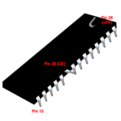
On each chip identify pin 20. The way to do this is to place the chip so that "U"-shaped notch is at the top. The pin in the top left corner (and left of the notch) is pin 1. The pin in the bottom left corner is pin 14. The pin in the bottom right corner is pin 15. The pin in the top right corner (and right of the notch) is pin 28.
Therefore pin 20 is the sixth pin from the bottom on the right side of the chip.
Having identified pin 20 you need to bend it up so that it sticks out at right angles (or more) to the chip's body (a wacky move huh!). Do this for both chips.
Now you need to piggy back the two chips so that they are both the same way up (both with the "U"-shaped notch at the top for example), and exactly aligned so that pin 1 on one chip is in contact only with pin 1 on the other.
Once you have tried this out and got it right, you may find the next stage easier if you glue the bodies (not the pins) of the two chips together. Don't use something which sets too quickly. You want to have a chance to slide a chip so that they are both correctly aligned.
You now need to solder each pair of pins together for all pins except pin 20 (ie pin 1 to pin 1, pin 2 to pin 2 etc. etc.). There is a possibility that you might overheat the chip if you do this carelessly. Use a small electronic technician's soldering iron and fine (0.7mm dia.) rosin cored solder. Do not use a blow torch and plumber's solder, oxyacetylene torch, MIG welder, thermic lance or other inappropriate tool.
If you want to be really careful, make each connection quickly and then allow the chip to cool for a while before making the next. You could also zig zag around the pins instead of doing them in consecutive order.
Once you have soldered each of the pin pairs your chips should look something like this:
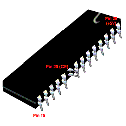
Call the top chip "RAM1" and the bottom chip "RAM2".
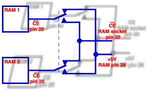
Get some fine single core wire (I used "wire-wrap" wire), and wire the switch as per these diagrams:
 |
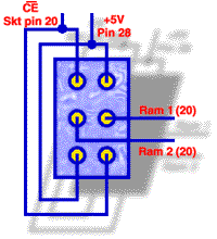 |
What you are doing is arranging the pin 20 on each chip so that, with the switch in one position, RAM1 is connected to the chip enable buss on the PCB, while RAM2 is connected to +5 Volts, then when the switch is in the other position RAM1 is connected to +5 Volts and RAM2 is connected to the chip enable buss.
When the chip enable pin on either RAM is connected to +5 Volts, that RAM effectively disappears from the circuit so that the Peavey PC 1600 only "sees" the other chip.
In order to pick up the chip enable buss from the socket, cut a pin off some other duff chip and solder a fine wire to the fat end of the pin. Solder the other end of the wire to the switch as per the circuit diagram above. To pick up the +5 Volts solder a fine wire to the top, fat end of pin 28 on RAM1.
Get hold of the wire from your switch with the chip pin on it and insert this pin into pin 20 of the RAM socket on the PC1600. Use the method described above to identify the pin. Pin 1 is at the battery end of the socket.
Then place the RAM sandwich into the socket in the normal way, making sure that all pins go into the socket, none are bent under, and that the "U"-shaped notch is closest to the battery. Also ensure that the two pin 20s on the RAMs and the wired pin inserted into the socket are not touching one another.
Mount your switch.
You will almost certainly be unable to close the box, because the extra height of the RAM sandwich is jamming it open. Using a fine round needle file, extend the six holes in the top panel downwards into open ended slots.
Now line up the screw holes in the base panel with the open end of slots in the top panel and screw down tight.
Initialise the PC1600 according to the instructions above then read the following section "In Use".
Now sing for joy - your Peavey PC1600 is "twice the size of the other gize" (Unless they've read this page too.)
It is possible, depending on what switch type you use, that both chips could momentarily get enabled at the same time resulting in a buss conflict. For this reason you might want to be cautious and always switch memory banks with the power off. I haven't experienced any problems of this sort, so I generally don't bother.
If you do switch banks with the power up, you may want to reselect the preset, this makes sure that the display (which has its own separate memory buffer) is updated and reports the name and number of the current preset correctly. Even if you don't do this any new fader/button motions will be correctly displayed.
In addition to the two sets of presets, two sets of scenes etc., don't forget that you have two sets of MIDI channel settings, delays, program maps etc in the "Utilities" settings. If you use the global channel/device number features of the PC1600x, remember that each of your "two" PC1600s has a separate setting for these, and you should line up any presets which use them into the correct one of your "two" PC1600s.
Any other developments will go here.
End of document updated 30th. September 1999
Godric Wilkie